Descriptions
Introduction to Semiconductor Process 2, Offered by Korea Advanced Institute of Science and Technology (KAIST). This course provides a general understanding of advanced semiconductor processes, focusing on physical principles, fabrication steps, and applications in modern electronics. You will learn about epitaxy, ion implantation, advanced photolithography, plasma etching, and chemical vapor deposition. Through practical examples and real-world analysis, you will gain foundational knowledge for further study or work in electronics, materials science, and semiconductor engineering.
What you’ll learn
- Understand the physical principles behind advanced semiconductor processes
- Learn the main steps of advanced semiconductor device fabrication
- Explore techniques such as epitaxy, ion implantation, advanced photolithography, plasma etching, and chemical vapor deposition
- Apply process knowledge to real-world semiconductor manufacturing
- Build a foundation for advanced study or work in semiconductor engineering and materials science
Who this course is for
- Students and professionals interested in advanced semiconductor processing
- Electronics and materials science majors
- Anyone seeking a solid introduction to advanced semiconductor manufacturing
Specificatoin of Introduction to Semiconductor Process 2
- Publisher : Coursera
- Teacher : Keon Jae Lee
- Language : English
- Level : Intermediate
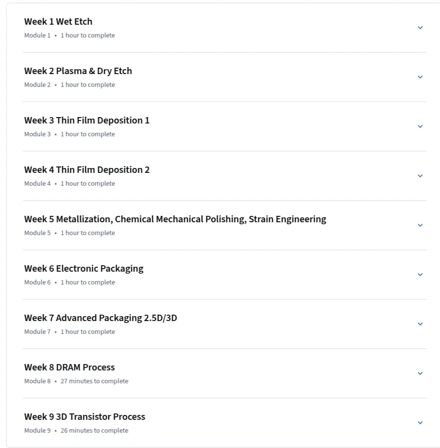
- Number of Course : 9
- Duration : 6 hours to complete
Content of Introduction to Semiconductor Process 2

Requirements
- No background is required ; all are welcome
Pictures
Sample Clip
Video Player
00:00
00:00
Installation Guide
Extract the files and watch with your favorite player
Subtitle : English
Quality: 720p
Download Links
Downloadly
Rapidgator
Password file(s): www.downloadly.ir
File size
384 MB