Descriptions
Mastering PCB Design and Layout Specialization, This specialization is designed for those looking to master the entire PCB design process, from schematic creation to generating manufacturing files. You will learn to translate a product concept into a functional schematic, select the right components, and create a comprehensive bill of materials. The curriculum covers the fundamentals of PCB layout, including component placement, routing strategies for signal integrity, and managing power and ground planes. You will gain hands-on experience with industry-standard CAD tools and learn to apply best practices for creating professional, manufacturable circuit boards.
Through a series of focused courses, you will delve into advanced topics such as Design for Manufacturing (DFM) and Design for Test (DFT) to ensure your designs are not only functional but also cost-effective and reliable. The program emphasizes practical skills, teaching you how to handle high-speed signals, minimize noise, and prepare a complete documentation package for fabrication and assembly. By the end of this specialization, you will have the expertise to design complex PCBs, troubleshoot layout issues, and confidently take a product from concept to production.
What you’ll learn
- Understand the complete PCB design workflow from schematic to layout and manufacturing.
- Learn to create detailed schematics and select appropriate electronic components.
- Master component placement and signal routing techniques for optimal performance.
- Apply Design for Manufacturing (DFM) and Design for Test (DFT) principles.
- Manage power distribution and grounding to ensure signal integrity.
- Prepare a full documentation package for PCB fabrication and assembly.
Who this course is for
- Aspiring PCB designers and hardware engineers.
- Electrical engineering students and hobbyists.
- Software engineers who want to understand hardware design.
- Professionals looking to formalize their PCB layout skills.
- Anyone interested in turning electronic concepts into physical products.
Specificatoin of Mastering PCB Design and Layout Specialization
- Publisher : Coursera
- Teacher : Starweaver
- Language : English
- Level : Intermediate
- Number of Course : 3
- Duration : 4 weeks to complete at 10 hours a week
Content of Mastering PCB Design and Layout Specialization

Requirements
- Basic electronics knowledge and familiarity with circuits
Pictures
Sample Clip
Installation Guide
Extract the files and watch with your favorite player
Subtitle : English
Quality: 720p
Download Links
Downloadly
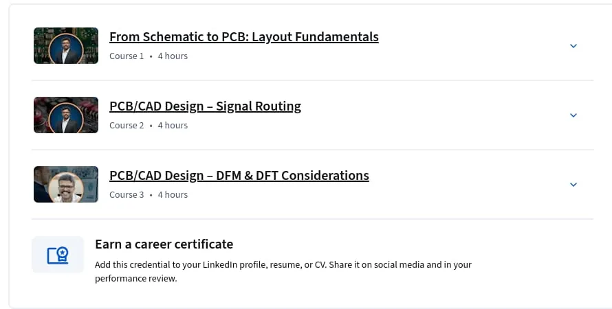
Course 1 – From Schematic to PCB: Layout Fundamentals
Course 2 – PCB/CAD Design Signal Routing
Course 3 – PCB/CAD Design DFM & DFT Considerations
Rapidgator
Course 1 – From Schematic to PCB: Layout Fundamentals
Course 2 – PCB/CAD Design Signal Routing
Course 3 – PCB/CAD Design DFM & DFT Considerations
File(s) password: www.downloadly.ir
File size
1.75 GB